 070-4121-5539


Semiconductor OSAT Package & Electrical Test Services

Semiconductor OSAT Package & Electrical Test Services

Semiconductor OSAT Package & Electrical Test Services

SNPT is committed to client success as our driving force for growth.
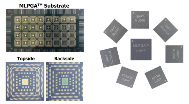
Substrate-based PKG designed to match JEDEC L/F dimensions for SMT, enabling rapid response within 3-4 days during early development.
6, 8 & 12” Wafers and Bumped Wafers
Particle Management (Class 1K)
Unit(Manual) Marking & Remarking
(Any type PKG)
Mass Marking (1000K/monthly)
Proprietary versatile semiconductor package designed and developed for custom customer specifications.

SNPT is committed to client success as our driving force for growth.

All semiconductor solutions available in one place.

Extensive experience and technical know-how.

Strict quality assurance and rapid turn-around time.

Optimal cost-effective semiconductor solutions.

Reliable partnership based on trust and sincerity.
Contact SNPT anytime if you have any questions.


Mon-Fri am 9:00 - pm 6:00
(Lunch 12:00 - 13:00)
070 - 4121 - 5539
010 - 3342 - 7062
Contact SNPT anytime if you have any questions.

 070-4121-5539